Introduction
JTAG is an integrated method for testing interconnects on printed circuit boards (PCBs) that are implemented at the integrated circuit (IC) level. Since its introduction as an industry standard in 1990, JTAG has continuously grown in adoption, popularity, and usefulness—even today, new revisions and supplements to the IEEE Std.-1149.1 standard are being developed and implemented. This document is a brief introduction to the nature and history of JTAG, from its introduction to new extensions in current development.
JTAG Technology
JTAG is commonly referred to as boundary-scan and defined by the Institute of Electrical and Electronic Engineers (IEEE) 1149.1, which originally began as an integrated method for testing interconnects on printed circuit boards (PCBs) implemented at the integrated circuit (IC) level. As PCBs grew in complexity and density—a trend that continues today—limitations in the traditional test methods of in-circuit testers (ICTs) and bed of nails fixtures became evident. Packaging formats, specifically Ball Grid Array (BGA) and other fine pitch components, designed to meet ever-increasing physical space constraints, also led to a loss of physical access to signals.
These new technology developments led to dramatic increases in costs related to designing and building bed of nails fixtures; at the same time, circuit board test coverage also suffered. JTAG/boundary-scan presented an elegant solution to this problem: build functionality into the IC to assist in testing assembled electronic systems.
Today, JTAG is used for everything from testing interconnects and functionality on ICs to programming flash memory of systems deployed in the field and everything in-between. JTAG and its related standards have been and will continue to be extended to address additional challenges in electronic test and manufacturing, including test of 3D ICs and complex, hierarchical systems.
History of JTAG
In the 1980s, the Joint Test Action Group (JTAG) set out to develop a specification for boundary-scan testing that was standardized in 1990 as the IEEE Std. 1149.1-1990. A few years later in 1993, a new revision to the standard—1149.1a—was introduced to clarify, correct, and enhance the original specification. An additional supplement, 1149.1b, was published in 1994 to add Boundary-Scan Description Language (BSDL) to the standard, paving the way for fast, automated test development and spurring continuous adoption by major electronics producers all over the world. The lessons that were learned became formalized in an update to the core standard in 2001 and IEEE-1149.1-2001 was published.
As new applications of JTAG were discovered, new standards were developed to extend the capabilities of JTAG. Standards such as the IEEE-1149.5 module test and maintenance bus standard in 1995 and the IEEE-1149.4 standard for mixed-signal testing in 1999 were met with low adoption rates and are not widely used at present. The IEEE-1149.6 standard introduced in 2003, on the other hand, began with slow adoption but has since become standard in many ICs as the technology it addressed—high-speed, AC-coupled signals—became a common feature of electronic systems. IEEE-1149.7, published in 2009 to address the need for JTAG in low-pin-count systems, is now standard on many popular microcontrollers.
Additional standards have also been published to add specific test capabilities. In 2002, the IEEE-1532 standard for in-system configuration of programmable devices was released and is now a common feature of FPGAs and their supporting software systems. IEEE-1581 was developed in 2011 to provide a convenient method of testing interconnects of high-speed memories with slow-speed test vectors; a version of this capability is implemented in some DDR4 memory components. To address the new application of combined capacitive sensing and boundary-scan test, IEEE-1149.8.1 was published in 2012. The extensibility of JTAG has been proven time and again.
More recently, efforts have been made to standardize JTAG access to instruments embedded within ICs. The IEEE-1149.1 standard was updated once more in 2013 for some housekeeping and to add extensions to access these instruments. Just one year later, an alternative standard for accessing these instruments, IEEE-1687, was published. Looking to the future, industry activities to extend JTAG into 3D-IC testing, system-level testing, and high-speed testing are already underway, proving that the versatility and extensibility of JTAG is here to stay.
How Does JTAG Work?
The JTAG/boundary-scan test architecture was originally developed as a method to test interconnects between ICs mounted on a PCB without using physical test probes. Boundary-scan cells created using multiplexer and latch circuits are attached to each pin on the device. These cells, embedded in the device, can capture data from pin or core logic signals as well as force data onto pins. Captured data is serially shifted out through the JTAG Test Access Port (TAP) and can be compared to expected values to determine a pass or fail result. Forced test data is serially shifted into the boundary-scan cells. All of this is controlled from a serial data path called the scan path or scan chain.
Because each pin can be individually controlled, boundary-scan eliminates a large number of test vectors that would normally needed to properly initialize sequential logic. Using JTAG, tens or hundreds of test vectors may do the job that had previously required thousands. Boundary-scan enables shorter test times, higher test coverage, increased diagnostic capability, and lower capital equipment cost.
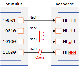
Two boundary-scan compliant devices are connected with four nets. The first device includes four outputs that are driving the four inputs of the other with predefined values. In this case, we assume that the circuit includes two faults: a short fault between Net2 and Net3, and an open fault on Net4. We will also assume that a short between two nets behaves as a wired-AND and an open fault behaves as a stuck-at-1 condition.
To detect and isolate defects, the tester shifts the patterns 3 into the first boundary-scan register and applies these patterns to the inputs of the second device.
Of course, interconnect testing is just one of many uses of JTAG—the aforementioned JTAG TAP has been extended to support additional capabilities including in-system-programming (ISP), in-circuit-emulation (ICE), embedded functional testing, and many more. The standard accounts for the addition of device-specific instructions and registers that can be used to interact with additional IC capabilities. For example, a microprocessor device may have embedded functionality for data download, program execution, or register peek-and-poke activities accessible using JTAG TAP; using the same tools, FPGA and CPLD devices can be erased, configured, read-back, and controlled using JTAG instructions through the IEEE-1532 standard. More recently, embedded IC instrumentation—from instruments that measure voltage and current to devices that can execute high-speed test on the chip—has used the JTAG TAP as the access mechanism, providing new visibility into the IC and further expanding the scope of JTAG testing.The input values captured in the boundary-scan register of the second device are shifted out and compared to the expected values. In this case, the results, underlined and marked in red on Net2, Net3, and Net4, do not match the expected values and the tester tags these nets as faulty. Sophisticated algorithms are used to automatically generate the minimal set of test vectors to detect, isolate, and diagnose faults to specific nets, devices, and pins.
JTAG for Product Life-Cycle Phases and Applications
While JTAG/boundary-scan was originally regarded as a method to test electronic products during the production phase, new developments and applications of the IEEE-1149.1 standard have enabled the use of JTAG in many other product life cycle phases. Boundary-scan technology is commonly applied to product design, prototype debugging, and field service.
The same test suite used to validate design testability can adapted and utilized for board bring-up, high-volume manufacturing test, troubleshooting and repairs, and even field service and reprogramming. The versatility of JTAG/boundary-scan tools delivers immense value to organizations beyond the production phase.

JTAG Test Basics
Most JTAG/boundary-scan systems are composed of two main components: a test program generator for test development and creation, and a test program executive for running tests and reporting results.
JTAG Test Program Generator
Test program generators accept computer aided design (CAD) data as input in the form of a netlist, bill of materials, schematic, and layout information. The test program generator (TPG) uses the information provided in these files, along with guidance from the test developer, to automatically create test patterns for fault detection and isolation using JTAG-testable nets on the PCB. Full-featured test program generation software will generally also include the capability to automatically generate tests for non-scannable components including logic clusters and memories that are connected to boundary-scan devices.
JTAG Test Program Executive
Test program executives are used to run the tests created by the test program generation software. The test executive interfaces with the JTAG hardware to execute test patterns on a unit under test (UUT), then compares the results with expected values and attempts to diagnose any failures. Modern test executives include advanced features such as flow control, support for third party test types, and often include an application programming interface (API) for integration with additional test systems or development of simplified operator interfaces.
JTAG Benefits
The continuous drive toward higher density interconnects and finer pitch ball-grid-array (BGA) components has fueled the need for test strategies that minimize the number of test points required. By embedding the test logic within the IC itself and limiting the physical interface to just a few signals, JTAG/boundary-scan presents an elegant solution to testing, debugging, and diagnosing modern electronic systems.
Today, JTAG provides the access mechanism for a variety of different system operations. Just some of the benefits provided by JTAG are:
Reuse through the product life cycle. The simple access mechanism provided by the JTAG TAP can be used at all stages of the product lifecycle—from benchtop prototype debugging to high volume manufacturing and even in the field.
Test point reduction. JTAG provides test access through just 4 pins (2 pins for IEEE-1149.7 compliant devices), reducing the number of test points required, resulting in lower PCB fabrication costs and reduced test fixture complexity.
Independent observation and control. Boundary-scan tests operate independently of the system logic, meaning they can be used to diagnose systems that may not operate functionally.
Extensibility. JTAG has seen continuous development and new applications are frequently being discovered. Additional standards have been developed to address AC-coupled testing, reduced pin counts, and control of test instruments embedded within ICs.

JTAG Scan Chain Infrastructure Test
JTAG testing usually begins by checking the underlying infrastructure to ensure that all devices are connected and test capabilities are operational. Test patterns are used to exercise the instruction register and boundary-scan register for comparison against expected lengths and values. If present, device ID codes can also be read and compared against expected values to ensure that the correct component has been placed.
JTAG Interconnect, Bus Wire, and Resistor Tests
After verifying that the scan chain is working properly, test patterns can be used to verify interconnectivity between system components. Nets that involve three or more boundary-scan pins represent a special case, called a bus wire, where additional patterns can be used to isolate faults to a specific pin. During a buswire test, boundary-scan driver pins are tested one at a time to ensure that all possible opens are tested.
Devices that are transparent to DC signals can be modeled as “short” signal paths and included in the test; for example, series resistors can be tested for component presence and open faults, while directional buffers can be constrained and tested to ensure that signals sampled at the buffer output pins match the signals that are applied to the buffer input pins. Additionally, tests for AC-coupled signals can be integrated with interconnect and buswire tests in systems with IEEE-1149.6 standard components, allowing capacitors to be tested for AC signal transparency.
Special tests can also be used to check pull-up and pull-down resistors, ensuring that resistors are present in the assembled system in addition to testing the nets for open and short faults. To accomplish this, resistors are tested by first driving the signal to a state opposite the pulled value. The net is then tri-stated, allowing the resistor to pull the signal back to the original state. Finally, the signal is sampled and the value is compared to the expected pulled value.
JTAG Testing in Logic, Memory, & Complex Devices
Not only can interconnections between boundary-scan components and simple transparent components be tested, but additional non-boundary-scan components can be controlled and tested for functionality and continuity using connected boundary-scan components. Simple test patterns may be used to test logic devices such as decoders or multiplexers, while sophisticated scripts may be used control and test complex devices for basic or advanced functionality, including analog-to-digital converters, UARTs, and Ethernet PHYs.
A common application of a cluster tests uses the storage capability of RAM devices to verify interconnects between a boundary-scan device and a connected memory. Using a model of the memory component, tests can be automatically created to write specific data patterns to memory addresses and then read back and compared against the expected value. These patterns are designed to ensure that all memory data and address signals are driven to both high and low logic states. The same concept used to test RAM can also be applied to non-volatile memory, such as flash, EEPROM, and NVRAM components.
JTAG Testing throughout Product Lifecycle
While JTAG/boundary-scan was originally regarded as a method to test electronic products during the production phase, new developments and applications of the IEEE-1149.1 standard have enabled the use of JTAG in many other product life cycle phases. Boundary-scan technology is commonly applied to product design, prototype debugging, and field service.
The same test suite used to validate design testability can adapted and utilized for board bring-up, high-volume manufacturing test, troubleshooting and repairs, and even field service and reprogramming. The versatility of JTAG/boundary-scan tools delivers immense value to organizations beyond the production phase.
JTAG Embedded Test
Many modern processors use JTAG as the main interface for on-chip debugging (OCD), allowing the processor to be controlled over the JTAG port within an embedded system.
Using this same interface, the JTAG port can be used to initialize a processor, download and run a test program, and then obtain results; this test technique is a fast, convenient method for developing and executing peripheral tests and in-system-programming operations in embedded systems.
Because these tests run at the system processor speed, defects that may not be identified during low-speed execution can be detected.
For more information see this video: https://www.youtube.com/watch?v=Netxo6NZ2Ws
In-System-Programming with JTAG
In addition to test applications, JTAG is also frequently used as the primary method to program devices such as flash memory and CPLDs. To program flash devices, the pins of a connected boundary-scan-compatible component can be used to control the memory and erase, program, and verify the component using the boundary-scan chain. FPGA and CPLD devices that support IEEE-1532 standard instructions can be accessed and programmed directly using the JTAG port.
Faster performance can be achieved using a CPU or FPGA to program the flash. In these cases, a small flash programming application is downloaded to the controlling device over the JTAG port, which is then used to interface between the test system and the flash programming application running on the embedded system. The program can run at much higher speeds than boundary-scan, increasing production throughput and rivaling or surpassing the speeds of USB and Ethernet-based programming solutions, without requiring an operating system or high-level software be present on the embedded system.
The IEEE-1149.1 JTAG team had the foresight to design an extensible standard—one that could employ additional data registers for many different applications. As a result, JTAG has grown from its original roots for board testing into a ubiquitous port that can be used for diverse applications such as in-system-programming, on-chip debugging, and more recently control of instruments embedded within ICs.
Corporate Headquarters
Corelis, Inc.
13100 Alondra Blvd. Suite 102
Cerritos, CA 90703
Sales & General Inquiries
Toll-Free: 888.808.2380
Fax: 562.404.6196
Email: sales@corelis.com
Website: https://www.corelis.com/education/tutorials/jtag-tutorial/what-is-jtag/